Sunday, June 2, 2013
Switch Wiring Diagram Variationelectrical Online

Section 2 Using The Electrical Wiring Diagram The Basic Wire Color And.

Way Switch Wiring Diagram Variation 3 Electrical Online.

Really Good Illustration Of How A Switch Loop Is Wired.

Wiring For Double Light Switch Electrical Resource About.

And My Drawing Of The Newpro Tech Style Switch With Modification.
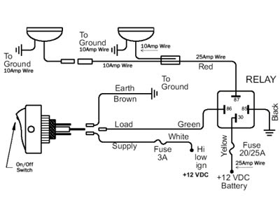
Photo Credit Toggle Switch Image By Sergey Danilov From Fotolia Com.

Line Diagram Of A Two Way Lighting Circuit Using Junction Boxes Fig 1.

Image Showing Wiring Diagram Of A One Way Light Circuit.

3989d1214628092 Wiring Diagram Three Way Switches Pilot Light 3 Way.

Is Basically A 3 Way Circuit With A 4 Way Switch Added Between The 2.
Saturday, April 13, 2013
Low Voltage Remote Mains Switch

Friday, April 12, 2013
Solid State Switch For Dc Operated Gadgets
Circuit diagram :
Author : Praveen Shanker
Wednesday, March 20, 2013
Automatic Switch For Voltage Converters
New applications for DC voltage converters, such as the ‘workhorse’ LT1070, arise every day. These converters can be adapted to nearly every imaginable ratio of input and output voltages. However, all of these circuits and devices have the same shortcoming, which is that they lack an on/off switch. Especially when they are used as a source of 6-V / 12-V power for a car radio, this is highly impractical. The circuit described here adds automatic load detection to the converter. For use in a car, the additional circuitry must be small and fit into a compact enclosure together with the converter. Since the battery voltage and ambient temperature vary over wide ranges, a simple form of load detection must be used. Besides this, the voltage drop across the load sensing circuitry must naturally be as small as possible. This can be achieved by using ‘ultra-modern’ SiGe technology.
The 6 V from the battery and the 12 V from the converter are combined in the MB R2545 dual diode. Consequently, a voltage of at least 6 V is always applied to the radio (for memory retention). If the radio is switched on, it draws a current from the 6-V battery, which may be around 100 mA.This current produces a voltage across R1. If this voltage is 75 mV or greater, the AC128 germanium transistor starts conducting and charges electrolytic capacitor C1, which is connected to the gate of the BUZ10. The MOSFET energises RE1 and thus connects the supply voltage to the converter. As a result, 12-V power is connected to the radio. The resulting increased current causes the voltage drop across R1 to increase, which is undesirable, so a 10-A Schottky diode is connected in parallel. The total voltage drop is thus approximately 0.6 V. The RC network connected to the BUZ10 ensures that the transistor always remains switched on for at least several seconds, to prevent the circuit from ‘chattering’ with varying current consumption.
Circuit diagram :

Automatic Switch For Voltage Converters
If the load is switched off, the AC128 cuts off, the electrolytic capacitor discharges and the relay again disconnects the voltage converter. The residual current consumption is so small that the circuit can also be connected ahead of the ignition switch. The Schottky diodes need only be rated for the necessary voltages and currents, and above all, they should have the lowest possible saturation voltage. The exact type is not critical. Two separate diodes can also be used. A small heat sink for the MBR diode won’t hurt, but this is normally not essential. Practically any type of PNP germanium transistor that is still available or on hand can be used (AC125, AC126 and AC128 work perfectly).
It may be necessary to modify the value of R1. In combination with the germanium transistor, R1 determines which level of current will be ignored (for memory retention) and which level of current will cause the converter to be switched on. With the component values shown in Figure 1, this level is between 10 mA and 25 mA. It is recommended to measure the quiescent current (at 6 V) and switch-on current of the load and then simulate the switching process using dummy load resistors. When selecting the 6-V relay, ensure that its contacts have an adequate current rating. The actual value can be significantly greater than the nominal output current. With a load of 5 A at 12 V and a converter efficiency of 70 percent, the current through the relay contacts rises to 14.3 A.
Author: C. Wolff - Copyright: Elektor Electronics
Source : www.extremecircuits.net
Monday, March 18, 2013
Hard Disk Switch Circuit
In these times with viruses and other threats from the Internet it would be nice to have reassurance that the PC cannot be infected. That is why this circuit was designed. It makes it possible to install multiple hard disks inside the case of a PC, which are separated in such a way that viruses cannot move from one disk to another. In this case there are three drives installed, one for use of the Internet via ADSL, one for working with email and one for other applications. If data from the Internet never arrives on the third disk, it is effectively protected against viruses. The solution outlined here has been in satisfactory use for a couple of years. There is an additional benefit: if there are ever any problems with the operation of the computer, then it is very easy to change to another hard disk to check if the problem manifests itself there as well. In this case, fault finding can be made much easier. The circuit operates by only switching over the power supply voltages (5 V and 12 V) of the hard disks. The hard disk is out of service without a power supply. This works without a problem with S-ATA disks.
Circuit diagram:

Hard Disk Switch Circuit Diagram
With IDE disks this only works with modern drives. There may only be a combination of hard disks on the relevant port and no CD-ROM, DVD-drive, CD-burner or something similar. The selection of the desired hard disk is done with a rotary switch. This has to be set to the correct position before the computer is switched on. When the power supply is turned on, one of three relays is driven via diode D1, D2 or D3. The relays are provided with a hold circuit via a second diode (D4, D5 and D6). In this way the selected relay remains energised as long as the power supply voltage is present. After switching on, electrolytic capacitor C1 is charged via R1, so that the common contact of the rotary switch is quickly at 0 V. This prevents an accidental change of hard disk while the computer is in operation. The ADSL modem is powered from the PC. This power supply voltage is only present if hard disk number 2 is selected. This prevents the use of the Internet if one of the other disks is selected.
Author: Uwe Kardel - Copyright: Elektor Electronics Magazine
Friday, March 8, 2013
Make this Thermo Touch Operated Switch Circuit Using IC 741
Irrespective of the ambient conditions, our hands and fingers mostly exhibits some extra warmth or increase in the level of the temperature compared to the atmospheric levels.
This feature of our body has been exploited here for making this thermally activated touch switch circuit.
The proposed thermo-touch operated switch circuit has its own distinct advantages in contrast to the normal "touch resistance" based switches.
This design is not prone to humid areas, or wet conditions where normally a resistance based switch would falter and generate erratic results.
The circuit utilizes the ubiquitous 1N4148 diodes whose forward voltage drop alters by about 2 mV in response to a rise of 1 degree Celsius temperature over it.
Looking at the circuit diagram, when the diodes D3 and D4 are touched with the finger, the voltage at point A drops rapidly in comparison to point B, sufficient to make the output of the IC 741 change state.
The IC 741 has been configured as a comparator, and it compares the forward voltage drop of the diodes with respect to the reference voltage clamped at point B.
The output generates a TTL or a CMOS compatible logic pulse at point C, which can be easily used for triggering a flip flop circuit and an intended load.
P1 and P2 are the presets which may used for setting and optimizing the circuits response or the sensitivity.

Parts List
R1, R4 = 10K
R2, R3 = 56K
R5 = 1K
R6 = 1M,
P1 = 10K preset,
P2 = 1K preset
C1 = 104/ disc
T1 = BC547
IC1 = 741
D1----D4 = 1N4148